Overview:
A printed circuit board (PCB) mechanically supports and electrically connects electronic components or electrical components using conductive tracks, pads and other features etched from one or more sheet layers of copper laminated onto and/or between sheet layers of a non-conductive substrate. Components are generally soldered onto the PCB to both electrically connect and mechanically fasten them to it.
Objective:
The end objective of the development process is to launch onto the production line and into the market, a product that is cost effective, manufacturable, reliable, on time and unconditionally stable.
Pre-requisite:
The end objective of the development process is to launch onto the production line and into the market, a product that is cost effective, manufacturable, reliable, on time and unconditionally stable.
Duration:
40 Hours.- Introduction to Electronics
- Passive components
- Active components
- Multi Meter
- Component checking method
- Bread Board connections
- PCB Software tutorial
- PCB schematic design drawing
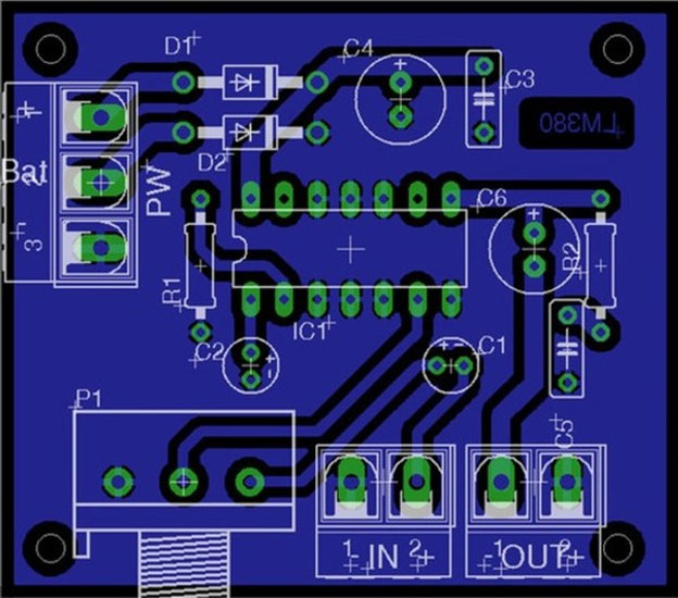
- PCB layout preparation
- PCB board Generation process
- Soldering process
- Output checking
Benefits of getting training with LCT
- Learning from certified instructors
- Program will be carried on both student and industrial basis
- Direct certification from MICROCHIP.
Course Outcome
- Trainee will have ability to work with PCB designing software.
- Trainee will have ability to draw the Electronic circuit.
- Trainee will have ability to generate the Real time PCB board
- Trainee will have ability to fixing component into PCB.
- Trainee will have ability to do Soldering process.